
|
Copyright 2001 IEEE. Published in the Proceedings of 35th Asilomar Conference on Signals, Systems, and Computers, Asilomar Hotel and Conference Grounds, Pacific Grove, CA, USA. November 4-7, 2001
The new generation of telecommunication equipment require the use of high order, high throughput Finite Impulse Response (FIR) filters. On the other hand, low power consumption is desirable for portable devices and ultra dense circuits. In this scenario, computationally intensive signal processing blocks can be effectively implemented by using the Residue Number System (RNS) arithmetic.
The use of the Residue Number System allows the decomposition of a given dynamic range in slices of smaller range on which the computation can be implemented in parallel [1], [2], [3]. The drawback presented by the RNS is the overhead due to both input and output conversions: binary to RNS, and RNS to binary. However, by using efficient conversion techniques [4], [5], the overhead can be significantly reduced.
In our work, we compare the performance, area and power of a FIR filter realized in the traditional binary system, with a RNS based one. Furthermore, we make the RNS filter faster than the traditional one by introducing a redundant carry-save representation, and on the other hand, we reduce the power dissipation of the plain RNS filter without affecting its delay by equalizing the parallel paths of the filter with a multiple supply voltage approach.
Results show that the RNS filter can sustain the same throughput as the traditional one, but dissipates less power. The carry-save RNS implementation of the filter can be clocked almost at double speed, with respect to the traditional one, without a significant increase in area and energy dissipated in a cycle.
The starting point of our design is a programmable N taps
FIR filter
|
|
|
In RNS, the FIR filter is decomposed into P filters working in parallel, as shown in Figure 2, and both binary to RNS and RNS to binary converters are required.
 |
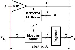
In each tap, a modular multiplier is needed to compute the term áak x(n-k)ńmi. Because of the complexity of modular multiplication, we used the isomorphism technique [6] to implement the product of residues By using isomorphisms, the product of the two residues is transformed into the sum of their indices which are obtained by an isomorphic transformation. According to [6], if m is prime there exists a primitive radix q such that its powers modulo m cover the set [1, m-1]:
|
|
|
Because of the transposed form of the FIR filter, the input x is the multiplicand of all the multiplications (see Figure 1). For this reason only one direct isomorphic transformation, incorporated in the binary to RNS conversion, is necessary for all the taps. On the other hand, because the coefficients of the filter (multiplicators) are constant terms loaded once at start-up, it is convenient to load directly the isomorphic representation modulo mi-1. As a result, in each tap, we reduce the modular multiplication to a modular addition, implemented as explained below, followed by an access to table (inverse isomorphism). The table is implemented as synthesized logic.
The modular addition
áb1 + b2 ńm,
consists of two binary additions. If the result
of b1 + b2 exceeds the modulo (it is larger than m-1),
we have to subtract the modulo m. In order to speed-up the operation
we can execute in parallel the two operations:
|
The resulting implementation of the tap for one modulo is depicted in
Figure 3. Due to the transposed form of the filter (Figure 1),
x must be buffered to avoid long delays.
The critical path of the RNS filter, given by the slowest modulo, is:
| (1) |
|
|
 |
In order to speed-up the operations by making the
clock period shorter, we can resort to a carry-save representation
for the binary representation of residues (ysk, yck) and
avoid to compute the modular addition in every tap.
The operands to be added in a tap are three: the product
pk = áak x(n-k)ńmi
and the carry-save representation of yk-1
|
| (2) |
However, the CS-representation implies the doubling of the registers,
and, as the number of taps increases, a logarithmic increase in the bit-width
of CSAs and registers. For this reason, it might be convenient to insert
some relay stations (RS), which assimilate the carry-save representation
of yk and extract its modulo mi, to prevent the bit-width from growing
too much.
Relay stations are depicted in Figure 5 and their delay is
| (3) |
The spacing of relay stations (i.e. the number n of taps between two
relay stations) can be determined by combining
Expr. (2), in which the term tbuffer increases with n,
and Expr. (3), where tcpa&mod depends on n.
However, by rewriting
tbuffer = tint + tload ·n,
the sum
|
|
 |
 |
In order to evaluate the performance of these RNS filters, we have implemented a N-tap error-free FIR filter (20 bits dynamic range) in the traditional two's complement system (T2S) [7], in RNS [7] and in RNS using the carry-save scheme (CS-RNS).
For the traditional T2S filter we opted for a carry-save representation in the taps to keep the cycle time as short as possible (Figure 6).
The product pk = ak x(n-k) is realized with a Booth multiplier [8] and the resulting partial products are accumulated in a Wallace tree structure which produces a carry-save representation of the product. Because the sum at the (k-1)-th tap Yk-1 = ĺi = 0k-1ai x(n-i) is stored in carry-save representation, an array of 4:2 compressors [9] is required to reduce the CS representation of pk and the CS representation of Yk-1 to the CS representation of Yk = Yk-1 + pk in the k-th tap.
The carry-save representation is finally converted into the two's complement representation by a carry-propagate adder (realized with a carry-look-ahead scheme) in the last stage of the filter.
The critical path is:
|
|
|
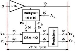 |
For the RNS and CS-RNS filters,
in order to have a dynamic range of 20 bits, as in the
case of the traditional implementation, we chose the following set of
moduli:
|
The multiplication was implemented with isomorphism in all the moduli but 3 (multiplication can be easily computed in tabular way) and 64 (modular product corresponds to the 6 least-significant bits of the conventional product).
Pipeline registers are added in the converters to maintain the clock cycle, determined by the critical path in the taps, to its minimum.
As for the implementation of carry-save RNS, in our design, the carry-save representation is not used for modulo 3 because its tap delay is sufficiently small. However, we have to place relay stations (just two 2-bit registers and, eventually, buffers) to synchronize áX ń3 with the other áX ńmi. For modulo 64, the use of CS-representation does not imply an increase of bit-width in the CSAs and registers.
For all the moduli, in our carry-save RNS (CS-RNS) filter we placed relay stations spaced by 8 taps, because this configuration gives us the best delay-area tradeoff.
The filters were implemented in a 0.35 mm library of Standard Cells. Delay, area and power dissipation have been determined with Synopsys tools.
The results are shown in Table 1 along with an evaluation of a possible implementation with multiple supply voltages (MV-RNS), described in the next section.
| ||||||||||||||||||||||||||||||||||||
In the table, area, reported as number of NAND2 equivalent gates, and power, computed at 100 MHz, are expressed as a function of the number of taps (N). Column N* indicates the N for which the RNS and the CS-RNS filter occupy less area and dissipate less power than the corresponding T2S filter. Although interconnections are not taken into account, local and global routing for the RNS is expected to be no worse than for the traditional filter.
In addition to the above presented implementations, we add a possible approach to reduce the power dissipation in a RNS filter without penalizing its speed.
The power dissipated in a cell depends on the square of the supply voltage (VDD) so that a significant amount of energy can be saved by reducing this voltage [10]. However, by lowering the voltage the delay increases, so that to maintain the performance this technique is applied only to cells not in the critical path.
Table 2 reports details on the implementation of the plain RNS filter for the different paths corresponding to the moduli mi. Delay is normalized to the critical path (i.e. clock cycle), while area and power dissipation are normalized to their per tap totals.
|
Because the single tap delay of moduli 3, 5, 7 and 64 is less than the critical path, we can use the available time slack and reduce the supply voltage for these moduli without affecting the overall performance.
In Table 3 we report the possible supply voltage which can be used in the modulo mi filters without increasing the critical path. The library of standard cells we used normally operates at VDD = 3.3 V. Table 3 also reports the power savings obtained with the listed supply voltage. These values have been computed assuming that the switching activity does not change when scaling the voltage. This assumption seems to be reasonable because an increased short-circuit energy, due to longer transition times, is compensated by a suppression of some glitches, due to a longer gate delay. The table shows a reduction of about 15% in the power dissipation per tap.
| |||||||||||||||||||||||||||||||||||||||||||||||||||||||||||||||
The use of a multiple supply voltage requires level-shifting circuitry when going from the lower voltage to the higher one [11]. In our case, voltage level shifters are only required for a few bits before the output conversion stage.
In this work, we compared the performance, area and power of FIR filters realized with the traditional binary arithmetic, the RNS, and the RNS with a carry-save representation of residues.
Table 1 shows that the RNS filter can sustain the same throughput as the traditional one, but dissipates less power for filters with more than 4 taps. The CS-RNS implementation of the filter can be clocked almost at double speed, with respect to the traditional one, without a significant increase in area and energy dissipated in a cycle (the power increases linearly with frequency). Finally, we showed a possible implementation of the RNS filter with multiple supply voltage, which can lead to an additional reduction of the power dissipated, without affecting the performance of the filter.
This work was partially supported by MURST project: Codesign methods for low power integrated circuits.