
Dept. of Electrical Engineering, University of Rome "Tor Vergata", Rome, Italy *Dept. of Informatics & Math. Modelling, Technical University of Denmark, Kongens Lyngby, Denmark
The objective of the work described in [1] was the comparison of the power consumption of Finite Impulse Response (FIR) filters implemented in the traditional two's complement system (TCS) and in the Residue Number System (RNS). The work in [1] took into account the dynamic power dissipation, which was by far the dominant portion of the energy consumed a few years ago.
With the technology scaling, and the increased transistor's leakage due to sub-threshold currents, also the static power dissipation starts to play an important role in today's power budgets. Moreover, the increasing smaller CMOS transistors allow the hardware implementation of extra functions that before were executed in software, and the migration of complex system to portable devices. Because of the implementation of digital filters in ultra low power processors, such as the one used in tiny systems with limited available power, it is important the static power due to leakage is characterized and, possibly, reduced.
To have an idea of the impact of the device's leakage on power dissipation, we implemented a multiplier, which is the basic block of a FIR filter, in a 0.18 mm, a 0.12 mm and in a 90 nm library. We used the same timing constraint, the delay of 25 inverters with fanout of 4 (a standard measure of delay across different technologies) in their respective libraries. The results, shown in Table I, indicate that the power dissipation due to leakage Pstat increases both in absolute value and as the percentage of the overall power dissipation PTOT. By comparing the 0.18 mm and the 90 nm multipliers, we notice that PTOT has decreased of about 70% (mostly due to the scaling of VDD), but the static part Pstat has increased 14 times and its contribution to the total 40 times. Moreover, for the 90 nm implementation, if the multiplier is used as often as 1% of the processor usage time the static power dissipation becomes dominant. Therefore, the design of systems in nanometer technologies must take into account methodologies to reduce the static power dissipation.
In this work, we show that filters implemented in RNS, not only are convenient in terms of dynamic power dissipation (at the same operation rate), but also that the RNS is very effective in the reduction of the static power. In implementing these low power units, we take advantage of state-of-the-art design automation tools [2] which handle libraries of standard cells with dual threshold transistors [3].
|
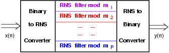
The use of alternative number systems in the implementation of application specific Digital Signal Processing (DSP) systems has gained a remarkable importance in recent years because of the lower power consumption over their two's complement counterparts.
A Residue Number System (RNS)
is defined by a set of relatively prime integers
|
|
| (1) |
|
In the RNS base, operations, such as addition and multiplication, are done in
parallel on the moduli
| (2) |
The conversion of the RNS representation of Z can be accomplished by
the Chinese Remainder Theorem (CRT):
| (3) |
Clearly, the conversions from N to RNS, and vice-versa, constitute a significant overhead in systems implemented in RNS. However, efficient methods to perform those conversions are presented in [7], [8], and [9].
A FIR filter of order N is described by the expression
| (4) |
|
|
As a direct consequence of (2), expression (4)
becomes in RNS:
| (5) |
|
 |
The standard cell library used provides two classes of cells: cells with devices with a reduced threshold voltage (Vt) designed to achieve high speed, identified in the following as HS, and cells with devices with a higher Vt to provide low leakage identified as LL [3].
Moreover, we consider the cells operating at the typical case conditions with a power supply VDD = 1.0 V and a temperature of 25 C.
By comparing the data-book for the two classes of cells HS and LL, the following points emerge when comparing the same cell (e.g. a NOT gate):
The total power dissipation for a CMOS gate is
| (6) |
| (7) |
The power due to short circuit currents Psc is
| (8) |
The term Pleak is the static power dissipation
| (9) |
In summary, LL cells are slower than HS cells, but dissipate less dynamic (if the switching activity is the same) and static power than the corresponding HS cells.
The current version of Synopsys Design Compiler [2] can handle the synthesis of dual Vt standard cell libraries such as the one described above. The prioritized design constraint is the delay (or better the clock period for a synchronous sequential system), but the tool keeps the power dissipation down by substituting HS cells with LL when there is a sufficient time slack. Moreover, the dynamic power dissipation is optimized as indicated in [11].
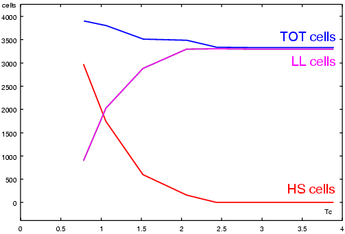
Figure 3 shows the variations in the HS and LL cell mix for a system synthesized with different values of the timing constraint TC. In the circuit synthesized with the smallest TC (minimum delay), the number of HS cells is dominant over the LL cells. For the circuit synthesized with a longer TC (right side of Figure 3), all cells are of LL type to have a reduced power dissipation.
 |
The objective of the work is the reduction of the overall power dissipation without affecting the throughput of the filter, and to evaluate which of the techniques used for the reduction of the dynamic power dissipation are also beneficial for the static part.
Because each logic function can be implemented with a HS or a LL cell, the first idea is to replace faster and power hungrier HS with LL cells when possible. By the RNS decomposition of Figure 2, the filter is divided into as many independent clusters of cells as the RNS moduli. Because of the different size of the moduli, the clusters have different maximum delays. The available time slack in the faster clusters (smaller moduli) allows to exchange HS with LL cells and reduce both the dynamic and static power dissipation. This is similar to what is done in [12] in the dual voltage approach.
In order to compare the power dissipation of the filters, we have implemented a 16, 32 and 64-tap error-free programmable FIR filter (20 bits dynamic range, transposed form) in the traditional two's complement system (TCS) and in RNS.
Because FIR filters in transposed form are modular with respect to the number of taps (i.e. adding extra taps does not alter the filter architecture), for all the filters, we set as the main design constraint the same maximum delay (i.e. the critical path) which determines the filter's throughput.
The composing blocks of a FIR filter are multipliers, adders and registers. In the following, we describe the architectures chosen for implementing these composing blocks.
For the implementation of multipliers with the traditional binary system (TCS), we chose to keep the product in carry-save (CS) format in order to speed-up the operation, and delayed the assimilation of the CS representation to the last stage of the filter. For the FIR filter in transposed form (Figure 1), in each tap we need to add the CS representation of the product to the value stored in the register (previous tap). Again, to avoid the propagation of the carry, we can store the CS representation. For this reason, we need to implement the addition with an array of 4:2 carry-save adders (CSA), as shown in Figure 4.
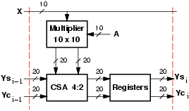 |
The CS representation is finally converted into the two's complement representation by a carry-propagate adder (realized with a carry-look-ahead scheme) in the last stage of the filter.
Figure 4 shows the implementation of the tap of a filter with programmable coefficients.
The critical path is
|
| (10) |
As already mentioned, a RNS filter can be decomposed, as shown in Figure 2, into P filters of smaller dynamic range (P is the number of moduli) working in parallel.
A key point in the design of the RNS filter is the choice of moduli.
To choose the set of co-prime numbers which cover the dynamic range of 20 bits, we
used the tool described in [13], which selects the set of
moduli giving the best delay/area/power tradeoffs according to the results
of the characterization of the RNS filter composing blocks.
Based on the tool, we chose for our RNS filters the following
set of moduli
|
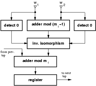
In each tap, a modular multiplier is needed and because of the complexity of modular multiplication, we used the isomorphism technique to implement the product of residues for prime moduli [4]. By using isomorphisms, the product of the two residues is transformed into the sum of their indices which are obtained by an isomorphic transformation (see [12] for implementation detail). The modular multiplication on mi = 64 is obtained by the normal binary multiplication limited to the 5 least-significant bits.
Figure 5 shows the implementation of a tap for a generic RNS prime
modulus.
The critical path for RNS filters in transposed form is the maximum delay
in the tap for the slowest modulus
|
|
The RNS FIR filter is completed by an input and an output conversion block.
Similarly to the TCS, the power dissipation in the RNS filter can be expressed
as a function of the filter order
| (11) |
 |
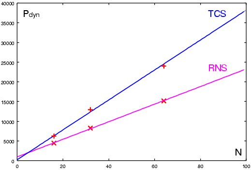
The comparison is carried out on filters implemented in the 90 nm STM library of standard cells (VDD = 1.0 V, at 25 C) [3], and the power dissipation has been computed by Synopsys Power Analyzer based on the annotated switching activity of random generated inputs. All the filters can be clocked at fmax = 500 MHz. Table II (upper part) summarizes the results for the implemented filters. The power dissipation is computed at a clock frequency of 100 MHz.
By interpolating the results for static, dynamic and total power dissipation, we obtain expressions of the power as a function of the filter order N (Table II, lower part) similar to those of (10) and (11). These trends are also plotted in Figure 6. The slopes [P/tap] indicated in Table II (lower part) represent the average power dissipated per tap.
From these results, it is clear that the RNS decomposition in parallel paths allows a reduction per tap of 40% for the dynamic and 50% for the static power without delay penalty (throughput). The area of the RNS filters is reduced as well.
| |||||||||||||||||||||||||||||||||||||||||||||||||||||||||||||||||||||||||||||
|

|
|---|
As the CMOS technology scales, a larger number of devices is integrated on a single chip, but the device's leakage has increased to a limit such that static power dissipation is no longer negligible.
In this work, we take advantage of the properties of the Residue Number System (RNS) to implement FIR filters with reduced static and dynamic power consumption.
The RNS decomposition in parallel paths allows an efficient use of libraries with HS cells, designed for high-speed, and LL cells, designed for low-power. In all the non-critical paths, the available time slack is used to substitute HS with LL cells resulting in a reduction of the power dissipation.
The implementation results show that the RNS filters offer a reduction of 50% in static power dissipation and a total power reduction of 40% with respect to the corresponding conventional filters.