|
Copyright 2003 IEEE. Published in the Proceedings of 2003 IEEE International Symposium on Circuits and Systems (ISCAS), Vol V, pages 413-416, Bangkok, Thailand, May 25-28, 2003.
In CMOS circuits the main contribution to power dissipation is the dynamic dissipation due to the charging and discharging of load capacitances. The well known expression P µ VDD2 CL a f shows the design parameters to change in order to modify the power figures of a system. We indicate with a the average activity of a circuit related to the clock frequency f (0 Ł a Ł 1). Usually the main constraint to be met in system design is the timing constraint (e.g. clock cycle). Therefore, reduction of power dissipation by lowering f is not implemented for these systems. On the other hand, lowering the supply voltage VDD, although it leads to a quadratic reduction of the power consumed, is also not implemented because the propagation delay of a circuit increase at a rate proportional to VDD/(VDD-VT)2 [1]. As a consequence, in most cases power optimization is carried out by minimizing the so called switching capacitance aCL: by reducing the switching activity in some parts of the circuit.
In a Residue Number System, defined by a set of relatively prime integers
{m1, m2, Ľ, mP} with dynamic range
M = Őmi,
any integer X Î { 0, 1, ĽM-1} has a unique
representation given by:
|
|
This parallelization usually implies a shortening of the critical path of a system, because narrower datapath have shorter carry chains and consequently smaller delays. Taking advantage of this parallelism, in [3] the power dissipation in RNS structures is reduced by lowering the supply voltage until the desired value of delay is obtained. In [4], we presented an approach to reduce power dissipation in a RNS filter without penalizing its speed. We used the time slack available in the non critical parallel paths and reduced VDD for these moduli until delays in all paths are equalized to the critical one. In this way, we reduce the power dissipation without affecting the overall performance. However, this multiple-VDD approach is very technology dependent and cannot be used if only one supply voltage is available for the whole chip, or it is not very effective if VDD cannot be easily scaled to the desired value.
In this work, we focus on power reduction techniques applied to the switching capacitance of RNS paths which are not the critical path. Our objective is to reduce the power dissipation without penalizing the overall performance.
Results show that reducing the switching capacitance, in some applications such as FIR filters, not only leads to more power efficient circuits, but also to better performance.
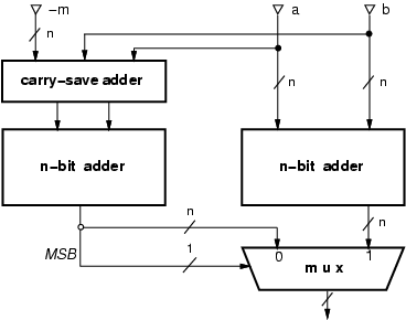
The modular addition
áa + b ńm,
consists of two binary additions. If the result
of a + b exceeds the modulus (it is larger than m-1),
we have to subtract the modulus m. In order to speed-up the operation
two additions are executed in parallel:
(a + b) and (a + b - m).
If the sign of the three-term addition is negative it means that
(a + b) < m and the modular sum is (a + b),
otherwise the modular addition is the result of (a + b - m).
The above algorithm can be
implemented with a carry-save adder (CSA),
two n-bit (n = élog2 mů)
adders1 (nCPA),
and a multiplexer
as shown in Figure 1.
|
|
The modular adder can be simplified when m = 2n (only a n-bit adder is required), and when m = 2n-1 (implemented with two n-bit adders in parallel, one with carry-in cin = 0 the other with cin = 1 and then selecting the correct result according to the cout computed in the adder with cin = 0).
In the general case of Figure 1, the delay of the modular adder is
|
The power dissipation is that of two additions executed in parallel.
We can reduce the power by switching off the path producing the unused
result in the modular adder of Figure 1 by predicting
if the binary sum of the two operands will exceed the modulus.
In this way, according to the prediction, we select the path
(left of right adder)
in the modular adder to be active and switch off the other. This
activation/deactivation can be done, for combinational logic, by using
transparent latches which block the propagation of the new values in
the adder to be turned off (Figure 2).
With this new scheme, the prediction function must be well chosen because
the delay of the resulting circuit is in the critical path as it is derived
from Figure 2:
|
|
It is clear, that the better the prediction function is, the smaller number of input combinations fall in case ENABLE BOTH.
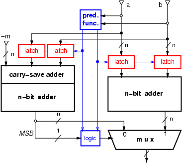 |
As an example, for m = 11 we can choose the following prediction function F
(indicating with a3 and a0 the MSB and the LSB of a, respectively):
|
|
For m = 11 and F defined above, in 40% of all possible input combinations the adder at right is enabled, in 27% the adder at left, and in 33% both adders are enabled. We implemented the original mod 11 adder and the new scheme, with a library of standard cells (0.35 mma,) by using Synopsys Design Analyzer, and obtained the following values for delay and power dissipation:
| delay [ns] | P [mW] | @ 100 MHz | |
| original | 1.45 | 440 | |
| new | 1.68 | 420 | |
| ratio | 1.15 | 0.95 |
The power reduction obtained (5%) in a favorable case (33% of ENABLE BOTH is quite good for a simple F) makes this techniques not very power efficient, although the delay overhead is not large and can be accommodated in a small time slack for RNS paths which are not critical. The introduced latches almost offset the reduced switching capacitance in the adders.
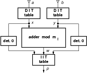 |
To reduce the complexity of modular multiplication, we use the
isomorphism technique [5] to implement the product of
residues.
This method works quite well for small prime moduli (m < 64).
By using isomorphisms, the product of the two residues is transformed
into the sum of their indices which are obtained by an isomorphic
transformation.
According to [5], if m is prime there exists a primitive
radix q such that its powers modulus m
cover the set [1, m-1]:
|
|
The tables are implemented as synthesized multi-level logic and
special attention has to be paid when one of the two operands is zero.
In this case there exists no isomorphic correspondence and the modular
adder has to be bypassed. The delay of the resulting scheme,
shown in Figure 3, is
|
 |
Because isomorph multipliers use modular adders in combination with tables, as a first step, we eliminate one of the adders in parallel and we incorporate the modulus reduction in the IIT table, as follows:
In this new scheme, depicted in Figure 4, the IIT tables are more complex (entries are doubled) than in the original scheme, but the delay is not increased because the multiplexer in the last stage of the modular adder is eliminated.
As a second step, we can incorporate the addition of the constant -mI in one of the DIT tables. The scheme of Figure 4 is modified as follows:
In this new scheme (Figure 5) we have eliminated the carry-save adder which was in the critical path, while the modifications in DIT* do not affect the table delay.
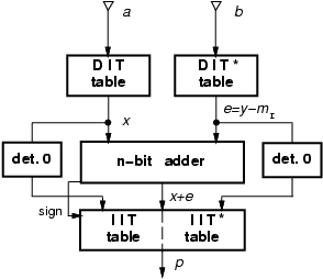 |
In conclusion, with this two modifications we reduced the critical path of
the isomorph multiplier to:
|
| delay [ns] | P [mW] | @ 100 MHz | |
| original | 2.00 | 535 | |
| new | 1.60 | 455 | |
| ratio | 0.80 | 0.85 |
For this isomorph multiplier the power is reduced by 15% and the delay of the new scheme is 20% shorter.
To evaluate the impact of the techniques presented above we implemented a 16-tap programmable FIR filter using different schemes:
|
In all schemes DIT tables can be eliminated because the input x is the multiplicand of all the multiplications and the DIT table is incorporated in the binary to RNS conversion, while the coefficients of the filter (multiplicators) can be directly loaded at start-up as isomorphism indices. We chose the set of moduli { 11, 13, 29 } which covers a 12-bit dynamic range.
Results in Table 1 show that the CS-filter is about 25% faster than the standard RNS, but consumes about 11% more power due the extra registers introduced to keep the carry-save representation of data. By implementing the new isomorph multiplier with reduced switching capacitance the power overhead is reduced to 5% and the speed-up with respect to the standard is 1.56 (about 37% faster).
We applied techniques aiming to reduce the switching capacitance to the design of modular adders and multipliers. For the adders, the power savings are quite small compared to the time overhead introduced. However, the technique of disabling some unused parts of a circuit by using transparent latches can lead to better results if those disabled parts are deeper (in terms of levels of gates) than adders, or if custom low-power latches are used.
The modifications introduced for isomorph multipliers allow a reduction both in delay and power dissipation and make very attractive the use of this modified multipliers in RNS FIR filters.
1Adders are implemented in a carry-look-ahead scheme. An extra inverter is required in the (a + b - m) adder to obtain the sign.
2 We implemented a multiplier which is used in FIR filters in which the DIT tables are eliminated as explained in the next section.