
Figure 1: Radix-4 combined division/square root unit.
| If you are unable to display correctly math fonts in Netscape under X11, click here. |
Alberto Nannarelli and Tomas Lang
Department of Electrical & Computer Engineering
University of California, Irvine, California 92697
e-mail : alberto@ece.uci.edu, tlang@uci.edu
Energy consumption is becoming more important every day because of the increased densities on chip and faster clocks. Although division and square root are infrequent operations, compared to addition and multiplication, because of their longer latency they dissipates a substantial part of the energy in floating-point units.
Because of the similarities in the algorithm it is quite common to implement division and square root in the same unit [4,,]. The purpose of this work is to implement a combined radix-4 division and square root floating-point double precision unit and to compare its performance and energy consumption with a radix-4 division only unit.
Previous work [9,,] has been done on reducing the energy dissipated in a divider. Here we are interested in evaluating the impact of the addition of the square root functionalities to the architecture presented in [9].
Techniques for the reduction of the power dissipation applicable to a variety of CMOS circuits are presented in [11,,], while others, specific for the algorithm in question, are presented in [9]. We apply those techniques to the combined division and square root unit and consider modifications and tradeoffs.
Results show that the energy dissipation for the combined division/square root unit can be reduced by about 35% without affecting the latency. An additonal 20% reduction is possible by using dual voltage. With respect to the radix-4 divider, the combined unit has a cycle time about 5% longer and a 15% higher energy consumption.
The units are implemented using the Passport 0.6 mm, 3.3 V, three-metal layers, CMOS standard cell library [3] and the layout is obtained by automatic floor-planning. The critical path is obtained from simulations, the area from the layout and the energy dissipation is estimated using PET [7], a power evaluation tool which computes the power dissipated in a circuit from the netlist extracted from the layout (that includes the effect of interconnection capacitance), the standard cell library energy views, obtained by characterization, and the results of a logic-level simulation. The simulation is run on a set of random-generated test vectors and stopped when a sufficient accuracy is reached in a Monte Carlo approach similar to the one presented in [1].
Because of the similarities in the algorithm, division and square root can be effectively implemented in the same unit. The radix-4 combined division and square root, described in detail in [4], is implemented by the residual recurrence
|
| (1) | ||||||||||||||
| ||||||||||||||
| ||||||||||||||||
|
The recurrence is implemented, as shown in Figure 1 with the selection function (SEL), the block to form F (FGEN), a block (DSMUX) which provides FGEN with the appropriate bit vector (depending on the operation), a carry-save adder (CSA), and two registers to store the carry-save representation of the residual. The conversion block performs the conversion from signed-digit to conventional representation and the rounding. The result is rounded in the last iteration according to the sign of the final residual and the signal that detects if it is zero, which are produced by the sign-zero-detection block (SZD).
The number of bits required in the recurrence is 55 fractional plus 1 integer for a total of 56 bits. To execute the operation 28 cycles are required for the iterations plus one additional cycle for the rounding, for a total of 29 clock cycles.
Figure 1: Radix-4 combined division/square root unit.
Block DSMUX selects the inputs to block FGEN according to the operation (division or square root) under execution. If the operation is a division, the value to provide to FGEN is d, while for square root the value to provide to FGEN is the partial result S[j] = A[j]. If in the conversion block we implement the algorithm described in [9], the value of B can be derived from A and the state in register C. In conclusion, in block DSMUX we utilize the inputs (d, A, and C) to obtain the desired outputs (AOUT, B) according to Table 1.
| op. | AOUT | B | ||||||||||
| div | d | d | ||||||||||
| sqrt | A |
| ||||||||||
| Zi refers to bit in position i in vector Z, being i = 0 the LSB. | ||||||||||||
The selection function can be divided into two parts: an adder and a logic function. The adder is an 8-bit carry-propagate adder whose addends are the 8 MSBs of the carry-save representation of W. The 7 MSBs of the sum are used to generate the result digit at each iteration, along with 3 bits of either d or A chosen as follows:
The selection logic function is described in Table 3. The digit h selected is the one satisfying the expression mh Ł [^y] < mh+1. The result digit is in the set {-2,-1,0,1,2} and four signals (M2, M1, P1, P2) are used to represent these five values in a one-out-of-four code (zero is coded as (0,0,0,0)). This representation makes the F-generator block (FGEN) simpler.
| 1 | 0 | - | first iteration (j = 0) |
| 1 | 1 | 1 | if (A < 0 > = 1) and (j > 0) |
| A < -2 > | A < -3 > | A < -4 > | if (A < 0 > = 0) and (j > 0) |
| A < -k > refers to bit in A with weight 2-k. A < -k > = A55-k | |||
| mh | dd, [^S][j] | |||||||
| [8/16] | [9/16] | [10/16] | [11/16] | [12/16] | [13/16] | [14/16] | [15/16] | |
|
m2 | 12 | 14 | 15 | 16 | 18 | 20 | 20 | 22 |
| m1 | 4 | 4 | 4 | 4 | 6 | 6 | 8 | 8 |
| m0 | -4 | -5 | -6 | -6 | -6 | -8 | -8 | -8 |
| m-1 | -13 | -15 | -16 | -17 | -18 | -20 | -22 | -23 |
| Values in table are multiplied by 16 | ||||||||
Block FGEN generates the signal F[j] as described in expression (1).
For square root the generation of F is quite complicated [4]. Table 4, where a...aa and b...bb represent bits of A[j] and B[j] respectively, shows the values of the bit-string for the different result digits. To keep track of the position, a 28-bit register (K) is used. The register K is initially loaded with 1 in the MSB and 0 in the remaining positions. At each iteration the 1 is replicated one position to the right according to the following expression.
|
|
| ||||||||||||||||||||||||||||||||||||
For division by setting all the bits of register K to 1 (all K1i = 1 and K2i = K3i = 0), F[j] can be generated by the same expression as for square root. This corresponds to
|
| sj+1 | F[j] | bit-string | ||||||||
| 27 | i+1 | i | i-1 | i-2 | 0 | |||||
| 0 | 0 | 00 | ... | 00 | 00 | 00 | 00 | ... | 00 | |
| 1 | -A[j]-2 ×4-(j+2) | [`a][`a] | ... | [`a][`a] | [`a]1 | 11 | 00 | ... | 00 | |
| 2 | -2A[j]-8 ×4-(j+2) | [`a][`a] | ... | [`a][`a] | 11 | 00 | 00 | ... | 00 | |
| -1 | B[j]+14 ×4-(j+2) | bb | ... | bb | b1 | 11 | 00 | ... | 00 | |
| -2 | 2B[j]+24 ×4-(j+2) | bb | ... | bb | 11 | 00 | 00 | ... | 00 | |
| K | 1 | ... | 1 | 1 | 0 | 0 | ... | 0 | ||
| K1 | 1 | ... | 1 | 0 | 0 | 0 | ... | 0 | ||
| K2 | 0 | ... | 0 | 1 | 0 | 0 | ... | 0 | ||
| K3 | 0 | ... | 0 | 0 | 1 | 0 | ... | 0 | ||
The minimum delay implementation, also referred as standard, is the one obtained with the constraint of minimum delay. The post-layout critical path is 7.3 ns. The critical path for the combined unit is 5% longer than the critical path for the division only unit of [9]. This is mainly due to the more complicated FGEN block.
In this section we apply the techniques described in [9] to the standard implementation. Because of the different conversion algorithm required for square root, with respect to the standard implementation of [9], in the combined unit a low-power conversion and rounding unit is already in place in the standard implementation. The other techniques applied are: retiming of the recurrence, change of redundant representation for the residual w[j], disabling of SZD, clock-gating of flip-flops in register K, and voltage scaling.
Retiming is the transformation that consists in re-positioning the registers in a sequential circuit without modifying its external behavior [6]. For the recurrence, the retiming is done by moving the selection function of Figure 1 from the first part of the cycle to the last part of the previous cycle (see Figure 2). A new 4-bit register is needed to store the result digit. The new register is initialized to q0 = 1 for division and s0 = 1 for square root.
This retiming causes a problem for the square root operation. The result digit sj+1 is converted in the next clock cycle and, as a consequence, in the first few iterations the value [^S][j] is not available for the selection function (Figure 3). However, because the digit-selection is done in the last part of the cycle and the conversion of the previous digit is a short delay operation, we can forward the value of the converted digit from the digit-converter to the the selection function and determine the correct value for [^S][j]. By indicating with s < 1 > s < 0 > the converted digit and with sSIGN its sign, Table 5 shows the modifications in the selection function.
By retiming the recurrence we reduce the switching activity in the F generator and in the CSA. Moreover, we change the critical path that is now limited to the eight most-significant bits, which allows the rest of the bits in the recurrence to be redesigned for low-power.

Figure 2: Retiming of the recurrence.
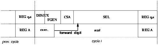
Figure 3: Digit forwarding.
| j | [^S][j] | ||
| 1,2 | A < 0 > | A < -3 > | A < 0 > |
| 3 | s < 0 > | 0 | 0 |
| 4 | A < -2 > ĹsSIGN | s < 1 > | s < 0 > |
| 5 | A < -2 > [`(([`(A < -3 > )] [`(A < -4 > )]sSIGN))] | A < -3 > [`(sSIGN)] +[`((A < -3 > ĹA < -4 > ))] sSIGN | A < -4 > ĹsSIGN |
| others | A < -2 > | A < -3 > | A < -4 > |
By using a radix-4 carry-save representation with two sum bits and one carry bit for each digit in the recurrence we only need to store one carry bit for each digit, instead of three. This can be done for the 48 LSBs that, after the retiming, are not on the critical path.
Furthermore, after the retiming, the eight MSBs, assimilated in the adder inside the selection function block, can be stored in wS eliminating another eight flip-flops in wC.
The sign-zero-detection block (SZD), which is only used in the rounding step, is switched off by forcing a constant logic value at its inputs during the recurrence steps.
Register K is used to generate F[j]. In division the register is initialized to 1 in each bit, and the configuration is not changed for the whole operation. In square root the register is initialized to 1 in the MSB and to 0 in the remaining bits. Every iteration the 1 is propagated to the next bit, for a total of two transitions per flip-flop (one to set the bit to 1, one to reset at the end of the operation). It is convenient to disable the clock for those flip-flops that do not need to be changed in a specific cycle. This is the same modification done for registers A and C in the convert-and-round unit implemented by gating the clock of the flip-flops not used [9]. The enabling function (for the i-th flip-flop) is
|
The power dissipated in a cell depends on the square of the voltage supply (VDD) so that significant amount of energy can be saved by reducing this voltage [2]. However, by lowering the voltage the delay increases, so that to maintain the performance this technique is applied only to cells not in the critical path. For example, in our library, designed to operate with VDD = 3.3 V, for VDD = 2.0 V the delay is doubled, and for voltages below 1.7 V the delay increases in excess. In the recurrence the 48 least-significant bits can be redesigned for low voltage. By using two voltages we only need to level-shift when going from the lower to the higher voltage [14]. As a consequence, the voltage-level shifters are not needed until a specific digit moves into the 8 MSBs.
Our library was designed to operate with VDD = 3.3 V.
In order to evaluate the possible lower voltage V2 to be used in a dual voltage implementation we need to determine the time slack available for the LSBs. The time slack is the difference between the delay in the paths through the MSBs and LSBs, and it gives the amount of time available for the delay of gates whose voltage is scaled to V2 (Table 6).
| MSBs: | DSMUX | FGEN | CSA | SEL | REG | ||
| 0.6 | 0.9 | 0.6 | 4.1 | 1.1 | = | 7.3 ns | |
| LSBs: | MUX | FGEN | CSA | REG | |||
| 1.2 | 0.9 | 0.6 | 1.1 | = | 3.8 ns | ||
The delay of the least-significant portion depends on the type of CSA adder used, since the delay of the radix-4 CSA is larger than that of the radix-2 CSA.
The critical path in the retimed implementation is 7.3 ns. By implementing the LSBs of the recurrence with radix-2 CSAs, the delay in the LSBs is 3.8 ns, resulting in a time slack of 3.5 ns. In this case V2 = 2.0 V without affecting the latency of the unit. On the other hand, by opting for the use of radix-4 CSAs, the time slack is reduced to 2.6 ns and, consequently, V2 can be lowered to 2.5 V.
Since the reduced voltage can be lower for radix-2 CSA, this might result in a reduction of the total energy. There is a tradeoff between the following:
Our estimation showed that the lowest energy is obtained by implementing radix-2 CSAs and V2 = 2.0 V for the dual voltage implementation.

Figure 4: Low-power combined division and square root unit.
The implementation that consumes a reduced amount of energy is shown in Figure 4. Table 7 reports the average energy dissipation and area for the standard and low-power implementation. In the Table, entry std refers to the standard implementation, optimized for speed, and entry l-p is the low-power implementation with the same delay. It was not possible to implement dual voltage with our cell library so that entry d-v is an estimate of a possible implementation.
The energy dissipation for the square root operation is about 10% lower than for the division, on average. This is due to the fact that for square root in every iteration we add F[j], which initially contains many zeros, to the residual w[j].
Some of the low-power techniques used, such as the changed redundant representation, reduce the number of flip-flops in the registers and, consequently, the area.
| division | sqr. root | |||||
| blocks | std | l-p | d-v | std | l-p | d-v |
| nJ | nJ | nJ | nJ | nJ | nJ | |
|
control | 0.9 | 0.9 | 0.9 | 0.9 | 0.9 | 0.9 |
| clk tree | 0.8 | 0.8 | 0.8 | 0.8 | 0.8 | 0.8 |
|
mux | 1.9 | 1.9 | 0.9 | 1.7 | 1.7 | 0.8 |
| DSMUX | 0.1 | 0.1 | 0.1 | 0.3 | 0.3 | 0.3 |
| FGEN | 7.3 | 4.9 | 2.4 | 5.8 | 4.3 | 2.0 |
| CSA | 8.8 | 5.2 | 3.8 | 4.7 | 3.9 | 2.3 |
| sel. func. | 1.5 | 2.0 | 2.0 | 1.2 | 1.8 | 1.8 |
| register Ws | 6.7 | 6.4 | *3.7 | 6.3 | 6.1 | *3.6 |
| register Wc | 6.7 | 2.7 | *3.1 | 5.1 | 2.2 | *2.5 |
| register q | - | 0.3 | 0.3 | - | 0.3 | 0.3 |
| register K | 1.3 | 0.0 | 0.0 | 1.6 | 0.5 | 0.2 |
|
SZD | 5.8 | 0.6 | 0.6 | 4.6 | 0.6 | 0.6 |
| C&R unit | 3.7 | 3.7 | *1.4 | 3.7 | 3.7 | *1.4 |
|
Eop [nJ] | 46.0 | 29.5 | 20.0 | 37.0 | 27.0 | 17.5 |
| Ratio to std | 1.00 | 0.65 | 0.45 | 1.00 | 0.75 | 0.50 |
| Esqrt/Ediv | - | - | - | 0.80 | 0.90 | 0.90 |
|
Area [mm2] | 1.9 | 1.8 | - | 1.9 | 1.8 | - |
| Values marked * include level shifters.
| ||||||
In this section we compare the results obtained for the radix-4 combined division and square root with those obtained in [9] for a radix-4 divider.
Table 8 summarizes the results for the implementation l-p when performing division. Similar blocks are put on the same row. The combined unit dissipates 15% more than the divider, in the average. The largest differences are for the blocks FGEN and "mux". The implementation of FGEN is considerably more complicated than the corresponding unit in the divider and gates with large number of inputs (8-input NAND) have been used to keep the number of levels of logic (and the delay) low. As for the multiplexer, in the retimed implementation of the divider, it is moved out of the recurrence. However, in the divider an extra cycle is required because the first iteration is only used for initialization and no quotient-digit is produced. In the combined implementation in the first iteration we perform the subtraction x-d using two inputs of the CSA and produce the first digit of the result.
|
blocks | divider | combined |
| control | 1.1 | 0.9 |
| clk tree | 0.9 | 0.8 |
| mux | 0.3 | 1.9 |
| DSMUX | - | 0.1 |
| FGEN | 2.8 | 4.9 |
| CSA | 4.8 | 5.2 |
| sel. func. | 1.6 | 2.0 |
| register Ws | 6.4 | 6.3 |
| register Wc | 3.5 | 2.7 |
| register q | 0.3 | 0.3 |
| register K | - | 0.0 |
| SZD | 0.6 | 0.6 |
| C&R unit | 3.9 | 3.7 |
|
Ediv [nJ] | 26.0 | 29.5 |
| Ratio | 1.00 | 1.15 |
| Area [mm2] | 1.2 | 1.8 |
| Ratio | 1.0 | 1.5 |
We have implemented a low-power radix-4 combined division and square root unit and compared performance and energy consumption with a radix-4 divider. We were able to apply the techniques presented in [9] to the combined unit obtaining a reduction of the energy of about 35% without increasing the latency. An additional reduction of 20% would be possible by using dual voltage. Furthermore, results show that the cycle time of the combined unit is 5% longer than the radix-4 divider and the energy dissipation is about 15% larger for the combined unit.
This work was partially supported by NSF grant MIP 9314172 and by State of California and Sun Microsystems, through UC MICRO 97-084.