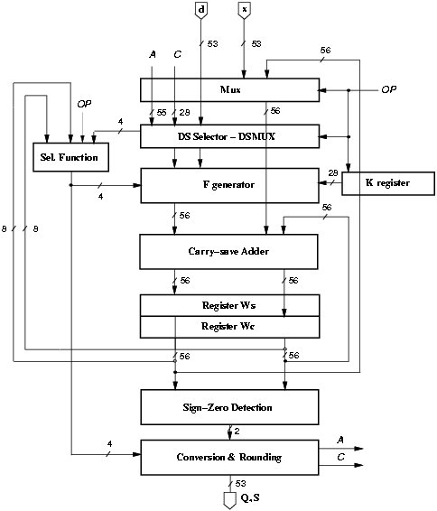
Figure 4.31: Radix-4 combined division/square root unit.
For radix-4, expression (2.6) and expression (2.7) are rewritten as
| (23) |
| (24) | ||||||||||||||
| ||||||||||||||||
|
The number of bits required in the recurrence is 55 fractional plus 1 integer for a total of 56 bits. To execute the operation 28 cycles are required for the iterations plus one additional cycle for the rounding, for a total of 29 clock cycles. The block diagram of the basic implementation is shown in Figure 4.31.
Figure 4.31: Radix-4 combined division/square root unit.
Block DSMUX selects the inputs to block FGEN according to the operation (division or square root) under execution. If the operation is a division, the value to provide to FGEN is d, while for square root the value to provide to FGEN is the partial result S[j], which coincides with A[j]. If in the conversion block we implement the algorithm described in Chapter 3 Section 3.10, the value of B can be derived from A and the state in register C. In conclusion, in block DSMUX we utilize the inputs (d, A, and C) to obtain the desired outputs (AOUT, B) according to Table 4.12.
| operation | AOUT | B | ||||||||||
| division | d | d | ||||||||||
| square root | A |
| ||||||||||
| Zi refers to bit in position i in vector Z, being i = 0 the LSB. | ||||||||||||
The selection function can be divided into two parts: an adder and a logic function. The adder is an 8-bit carry-propagate adder whose addends are the 8 MSBs of the carry-save representation of W. The 7 MSBs of the sum are used to generate the result digit at each iteration, along with 3 bits of either d or A chosen as follows:
The selection logic function is described in Table 4.14. The digit h selected is the one satisfying the expression mh Ł [^y] < mh+1. The result digit is in the set {-2,-1,0,1,2}. This representation makes the F-generator block (FGEN) simpler.
| 1 | 0 | - | first iteration (j = 0) |
| 1 | 1 | 1 | if (A < 0 > = 1) and (j > 0) |
| A < -2 > | A < -3 > | A < -4 > | if (A < 0 > = 0) and (j > 0) |
| A < -k > refers to bit in A with weight 2-k. A < -k > = A55-k | |||
| mh | dd, [^S][j] | |||||||
| 8/16 | 9/16 | 10/16 | 11/16 | 12/16 | 13/16 | 14/16 | 15/16 | |
|
m2 | 12 | 14 | 15 | 16 | 18 | 20 | 20 | 22 |
| m1 | 4 | 4 | 4 | 4 | 6 | 6 | 8 | 8 |
| m0 | -4 | -5 | -6 | -6 | -6 | -8 | -8 | -8 |
| m-1 | -13 | -15 | -16 | -17 | -18 | -20 | -22 | -23 |
| Values in table are multiplied by 16 | ||||||||
Block FGEN generates the signal F[j] as described in expression (2.7):
| ||||||||||||||
|
|
| |||||||||||||||||||||||||||
For division by setting all the bits of register K to 1 (all K1i = 1 and K2i = K3i = 0), F[j] can be generated by the same expression as for square root. This corresponds to
|
| sj+1 | F[j] | bit-string | |||||||
| 0 | j-1 | j | j+1 | j+2 | 27 | ||||
| 0 | 0 | 00 | ... | 00 | 00 | 00 | 00 | ... | 00 |
| 1 | -A[j]-2 ×4-(j+2) | [`a][`a] | ... | [`a][`a] | [`a][`a] | 11 | 10 | ... | 00 |
| 2 | -2A[j]-8 ×4-(j+2) | [`a][`a] | ... | [`a][`a] | [`a]1 | 10 | 00 | ... | 00 |
| -1 | B[j]+14 ×4-(j+2) | bb | ... | bb | bb | 11 | 10 | ... | 00 |
| -2 | 2B[j]+24 ×4-(j+2) | bb | ... | bb | b1 | 10 | 00 | ... | 00 |
| sj+1 | F[j] | bit-string | ||||||||
| 27 | i+1 | i | i-1 | i-2 | 0 | |||||
| 0 | 0 | 00 | ... | 00 | 00 | 00 | 00 | ... | 00 | |
| 1 | -A[j]-2 ×4-(j+2) | [`a][`a] | ... | [`a][`a] | [`a]1 | 11 | 00 | ... | 00 | |
| 2 | -2A[j]-8 ×4-(j+2) | [`a][`a] | ... | [`a][`a] | 11 | 00 | 00 | ... | 00 | |
| -1 | B[j]+14 ×4-(j+2) | bb | ... | bb | b1 | 11 | 00 | ... | 00 | |
| -2 | 2B[j]+24 ×4-(j+2) | bb | ... | bb | 11 | 00 | 00 | ... | 00 | |
| K | 1 | ... | 1 | 1 | 0 | 0 | ... | 0 | ||
| K1 | 1 | ... | 1 | 0 | 0 | 0 | ... | 0 | ||
| K2 | 0 | ... | 0 | 1 | 0 | 0 | ... | 0 | ||
| K3 | 0 | ... | 0 | 0 | 1 | 0 | ... | 0 | ||
The minimum delay implementation, also referred as standard, is the one obtained with the constraint of minimum delay. The post-layout critical path is 7.3 ns. The critical path for the combined unit is 5% longer than the critical path for the division only unit of Section 4.2. This is mainly due to the more complicated FGEN block. The energy dissipated by this basic implementation is shown in Table 4.19 in column ßtandard".
In this section we apply the techniques described in Chapter 3 to the standard implementation. Because of the different conversion algorithm required for square root, in the combined unit a low-power conversion and rounding unit, as the one described in Section 4.2, is already in place in the standard implementation. In addition to the techniques of Chapter 3, we reduce the energy dissipation in register K by gating the clock in the flip-flops.
The retiming is done by moving the selection function of Figure 4.31 from the first part of the cycle to the last part of the previous cycle (see Figure 4.32). The new 4-bit register is initialized to q0 = 1 for division and s0 = 1 for square root.
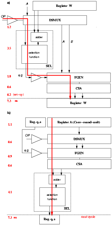
Figure 4.32: Retiming of the recurrence.
This retiming causes a problem for the square root operation. The result digit sj+1 is converted in the next clock cycle and, as a consequence, in the first few iterations the value [^S][j] is not available for the selection function (Figure 4.33). However, because the digit-selection is done in the last part of the cycle and the conversion of the previous digit is a short delay operation, we can forward the value of the converted digit from the digit-converter to the the selection function and determine the correct value for [^S][j].
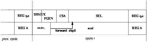
Figure 4.33: Digit forwarding.
By indicating with s < 1 > s < 0 > the converted digit and with sSIGN its sign, Table 4.17 shows the modifications in the selection function.
| j | [^S][j] | ||
| 1,2 | A < 0 > | A < -3 > | A < 0 > |
| 3 | s < 0 > | 0 | 0 |
| 4 | A < -2 > ĹsSIGN | s < 1 > | s < 0 > |
| 5 | A < -2 > [`(([`(A < -3 > )] [`(A < -4 > )]sSIGN))] | f1 | A < -4 > ĹsSIGN |
| others | A < -2 > | A < -3 > | A < -4 > |
| f1 = A < -3 > [`(sSIGN)] +[`((A < -3 > ĹA < -4 > ))] sSIGN | |||
After the retiming, we change the representation of the residual to reduce the number or flip-flops and use low-drive gates in the non critical portion of the recurrence as explained for the radix-4 divider in Section 4.2.
Register K is used to generate F[j]. In division the register is initialized to 1 in each bit, and the configuration is not changed for the whole operation. In square root the register is initialized to 1 in the MSB and to 0 in the remaining bits. Every iteration the 1 is propagated to the next bit, for a total of two transitions per flip-flop (one to set the bit to 1, one to reset at the end of the operation). It is convenient to disable the clock for those flip-flops that do not need to be changed in a specific cycle. This is the same modification done for registers A and C in the convert-and-round unit implemented by gating the clock of the flip-flops not used (Section 3.10.2). The enabling function (for the i-th flip-flop) is
|
| MSBs: | DSMUX | FGEN | CSA | SEL | REG | ||
| 0.6 | 0.9 | 0.6 | 4.1 | 1.1 | = | 7.3 ns | |
| LSBs: | MUX | FGEN | CSA | REG | |||
| 1.2 | 0.9 | 0.6 | 1.1 | = | 3.8 ns | ||
The critical path in the retimed implementation is 7.3 ns. By implementing the LSBs of the recurrence with radix-2 CSAs, the delay in the LSBs is 3.8 ns, resulting in a time slack of 3.5 ns. In this case V2 = 2.0 V can be chosen without affecting the latency of the unit. On the other hand, by opting for the use of radix-4 CSAs, the time slack is reduced to 2.6 ns and, consequently, V2 can be lowered to 2.5 V.
Our estimation showed that the lowest energy is obtained by implementing radix-2 CSAs and V2 = 2.0 V for the dual voltage implementation.
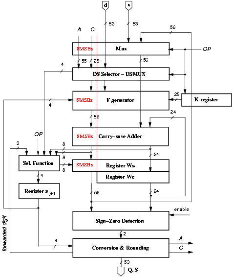
Figure 4.34: Low-power combined division/square root unit.
The synthesized selection function met the set delay constraints (3.0 ns). the reduction in energy dissipation, obtained by incremental compilation with energy dissipation constraints resulted to be about 25%, without increasing the delay.
The implementation that consumes a reduced amount of energy is shown in Figure 4.34. Table 4.19 reports the average energy dissipation and area for the standard and low-power implementation. In the table, entry std refers to the standard implementation, optimized for speed, entry l-p is the low-power implementation with the same delay, entry d-v is an estimate of a possible implementation with dual voltage, and entry sym is an estimate of l-p with selection function optimized by Synopsys Power Compiler.
The energy dissipation for the square root operation is about 10% lower than for the division, on average. This is due to the fact that for square root in every iteration we add F[j], which initially contains many zeros, to the residual w[j].
Some of the low-power techniques used, such as the changed redundant representation, reduce the number of flip-flops in the registers and, consequently, the area.
| division | sqr. root | |||||||
| blocks | std | l-p | syn | d-v | std | l-p | syn | d-v |
| nJ | nJ | nJ | nJ | nJ | nJ | nJ | nJ | |
|
control | 0.9 | 0.9 | 0.9 | 0.9 | 0.9 | 0.9 | ||
| clk tree | 0.8 | 0.8 | 0.8 | 0.8 | 0.8 | 0.8 | ||
|
mux | 1.9 | 1.9 | 0.9 | 1.7 | 1.7 | 0.8 | ||
| DSMUX | 0.1 | 0.1 | 0.1 | 0.3 | 0.3 | 0.3 | ||
| FGEN | 7.3 | 4.9 | 2.4 | 5.8 | 4.3 | 2.0 | ||
| CSA | 8.8 | 5.2 | 3.8 | 4.7 | 3.9 | 2.3 | ||
| sel. func. | 1.5 | 2.0 | 1.5 | 2.0 | 1.2 | 1.8 | 1.4 | 1.8 |
| register Ws | 6.7 | 6.4 | *3.7 | 6.3 | 6.1 | *3.6 | ||
| register Wc | 6.7 | 2.7 | *3.1 | 5.1 | 2.2 | *2.5 | ||
| register q | - | 0.3 | 0.3 | - | 0.3 | 0.3 | ||
| register K | 1.3 | 0.0 | 0.0 | 1.6 | 0.5 | 0.2 | ||
|
SZD | 5.8 | 0.6 | 0.6 | 4.6 | 0.6 | 0.6 | ||
| C&R unit | 3.7 | 3.7 | *1.4 | 3.7 | 3.7 | *1.4 | ||
|
Eop [nJ] | 46.0 | 29.5 | 29.0 | 20.0 | 37.0 | 27.0 | 26.5 | 17.5 |
| Ratio to std | 1.00 | 0.65 | 0.63 | 0.45 | 1.00 | 0.75 | 0.70 | 0.50 |
| Esqrt/Ediv | - | - | - | - | 0.80 | 0.90 | 0.90 | 0.90 |
|
Area [mm2] | 1.9 | 1.8 | - | - | 1.9 | 1.8 | - | - |
| Values marked * include level shifters.
| ||||||||
Figure 4.35 shows the breakdown, as a percentage of the total, of the energy dissipated in the main blocks composing the unit.
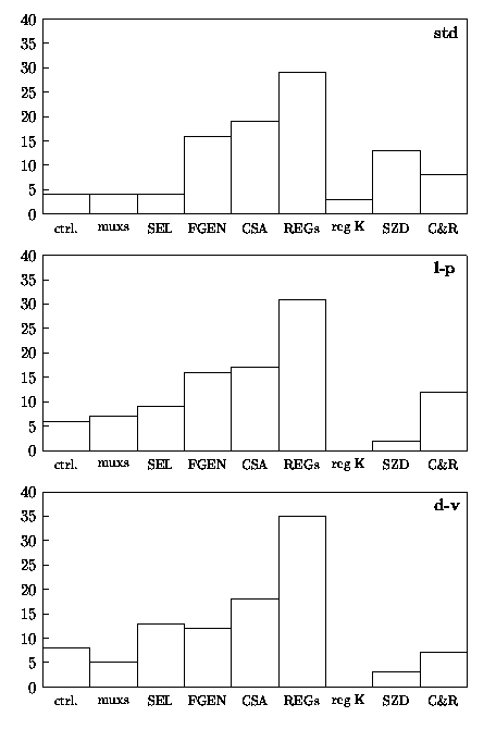
Figure 4.35: Percentage of energy dissipation in radix-4 combined unit.
In this section we compare the results obtained for the radix-4 combined division and square root with those obtained for a radix-4 divider.
Table 4.20 summarizes the results for the implementation l-p when performing division. Similar blocks are put in the same row. The combined unit dissipates 15% more than the divider, on average. The largest differences are for the blocks FGEN and "mux". The implementation of FGEN is considerably more complicated than the corresponding unit in the divider and gates with large number of inputs (8-input NAND) have been used to keep the number of levels of logic (and the delay) low. As for the multiplexer, in the retimed implementation of the divider, it is moved out of the recurrence. However, in the divider an extra cycle is required because the first iteration is only used for initialization and no quotient-digit is produced. In the combined implementation in the first iteration we perform the subtraction x-d using two inputs of the CSA and produce the first digit of the result.
|
blocks | divider | combined |
| control | 1.1 | 0.9 |
| clk tree | 0.9 | 0.8 |
| mux | 0.3 | 1.9 |
| DSMUX | - | 0.1 |
| FGEN | 2.8 | 4.9 |
| CSA | 4.8 | 5.2 |
| sel. func. | 1.6 | 2.0 |
| register Ws | 6.4 | 6.3 |
| register Wc | 3.5 | 2.7 |
| register q | 0.3 | 0.3 |
| register K | - | 0.0 |
| SZD | 0.6 | 0.6 |
| C&R unit | 3.9 | 3.7 |
|
Ediv [nJ] | 26.0 | 29.5 |
| Ratio | 1.00 | 1.15 |
| Area [mm2] | 1.2 | 1.8 |
| Ratio | 1.0 | 1.5 |