
Figure 1.1: Implementation of full-adder.
The functional blocks described in this appendix are those blocks common to most of the implementations presented in this work.
All the registers are implemented by using arrays of flip-flops. The flip-flops are D-type edge-triggered on the rising edge and include either SET pin, or RESET pin, or both.
The radix-2 carry-save adder is implemented as an array of full-adders. Each full-adder (FA) is implemented as depicted in Figure A.1 and it can be decomposed into two half-adders (HA). Its maximum delay is the delay of the two XOR gates, or half-adders (tFA = tHA + tHA).
Figure 1.1: Implementation of full-adder.
The selection function (SEL), except for radix-512, is usually composed by a small carry-propagate adder, because of the carry-save representation of the residual, and by a function implemented with logic gates as depicted in Figure A.2. The implementations of SEL are obtained by synthesis of the VHDL description of the selection function. SEL includes both the assimilation of the carry-save representation of [^y] and the actual digit-selection function.

Figure 1.2: Selection function.
The multiple generator (MULT) perform the following operation for division:
|
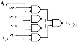
Figure 1.3: One bit of the multiple generator.
| digit | M2 | M1 | P1 | P2 |
| -2 | 1 | 0 | 0 | 0 |
| -1 | 0 | 1 | 0 | 0 |
| 0 | 0 | 0 | 0 | 0 |
| 1 | 0 | 0 | 1 | 0 |
| 2 | 0 | 0 | 0 | 1 |
To perform the rounding, it is necessary to detect the sign of the residual from its redundant representation and to determine if the residual is zero. In [10], a network to detect the two conditions: sign of residual, and residual is zero, is described. We now summarize its implementation. Let wS and wc be the values of the (h+1)-bit carry-save representation of the last residual. We introduce two quantities aS and aC such that
|
|
| (25) |
|
|
|
The subtraction of 2-h to the carry-save representation of w is done by adding a (h+1)-bit vector of 1s. The resulting expression for the bits of aS and ac are
| (26) |
The Pis of expression (A.2) are generated in a hierarchical way using a carry-look-ahead structure. For example, for a 64-bit sign-and-zero detection unit using groups of 4 bits we have the scheme of Table A.2. And the two corresponding expressions for zero and sign are:
|
|
|
|
| |||||||||||||||||||||||||||||||||||||||||||||||||
In this section we describe the voltage level shifter presented in [35]. Voltage level shifters are needed in circuits that operate with dual voltage (VDD regular supply voltage and V2 reduced supply voltage). Level shifters are necessary when a portion of the circuit at voltage V2 is connected to a portion at voltage VDD. As shown in Figure A.4, if the output of a circuit operating at V2 (C2) is connected directly to the input of a circuit operating at VDD (C1), static current flows in C1 at the input level "high". Since the voltage of node N1 is not raised higher than V2, the p-transistor MP1 cannot be cut-off if V2 < VDD - Vthreshold,p . Therefore, static current flows from VDD to VSS through MP1 and MN1. In order to block this static current a voltage level shifter is inserted at node N1. No level shifting is necessary when, in the reversed case, the output of a VDD operated circuit is connected to the input of a V2 circuit. The voltage level shifter is realized as depicted in Figure A.5. Table A.3 indicates the input-output delays and energy consumption for a level shifter operating at VDD = 3.3 V and V2 = 2.0 V, and its comparison with an inverter of the Passport library. The values in Table A.3 were obtained by SPICE simulation.

Figure 1.4: Dual voltage: C1 is not cut-off.
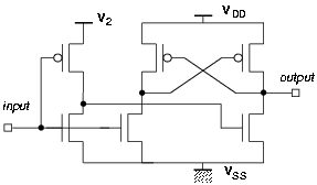
Figure 1.5: Voltage level shifter.
| level shifter | inverter | |||||||||
| delay [ns] | Etran | delay [ns] | Etran | |||||||
| tLH | trise | tHL | tfall | [nJ] | tLH | trise | tHL | tfall | [nJ] | |
| SL1 | 0.144 | 0.13 | 0.042 | 0.11 | 0.7 | 0.097 | 0.20 | 0.094 | 0.16 | 0.3 |
| SL4 | 0.245 | 0.17 | 0.087 | 0.22 | 1.2 | 0.164 | 0.32 | 0.163 | 0.27 | 0.8 |
| SL16 | 0.670 | 0.45 | 0.271 | 0.69 | 3.4 | 0.459 | 0.98 | 0.476 | 0.86 | 2.1 |
| SL = standard load = 22 fF for Passport library | ||||||||||