Figure 2.1: Structure of PET.
In this appendix we describe the features of some CAD tools used in the realization of this work. A brief description of COMPASS tools is given in Chapter 4. First, the two tools developed in our laboratory (PET and ACC) are presented. Then, the main features of the commercial tool Synopsys Power Compiler are summarized.
PET belongs to the category of power estimators loosely-coupled with the simulator. It is coupled with COMPASS Qsim and it was developed internally for two main reasons:
PET computes the energy and power dissipation by reading the energy views for the cells in the library, the layout-extracted netlist and the trace file generated by Qsim. The energy views are computed once for a given library, by characterization using ACC (Section B.2), and then stored in a database.
As discussed in Section 1.2, the energy consumption in a cell is proportional to the output load, the supply voltage, the number of output transitions in a given time window and the energy dissipated internally. This is summarized by expression (1.5), which is rewritten below
|
The term between parenthesis
|
|
as
|
In a sequential cell also the internal switching, not affecting the cell's output, dissipates energy. To take into account this contribution we can write the energy and power expressions in the following way:
|
|
Now we consider a large circuit containing N cells, NS of which are sequential. The total energy consumption in the time window is given by:
| (27) |
Summarizing, in order to calculate the energy dissipated, given by expression (B.1) we need to determine the value of the following parameters:
To compute the power dissipation
| (28) |
The quantities VDD, Eint and Ecl depend on the library that we are using. CL depends on the design and layout (type of cell connected and wire capacitance) and the number of transitions depends on the design and on the set of input vectors used.
The procedure to determine the energy and power dissipation is the following:
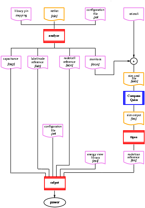
The procedure described above was implemented in PET. It consists of three C routines (analyze, ttgen and calpot) and the use of two COMPASS tools: Qsim (logic-level simulator) and extract (COMPASS Interconnect layout to netlist extractor) [38]. The latter is used to determine the capacitance (including wires) at each node of the circuit while Qsim is used to determine the logic values of the nodes used later to determine the number of transitions. PET is structured as depicted in Figure B.1.
Figure 2.1: Structure of PET.
analyze reads the extracted netlist and determines the output load for each cell of the circuit. It also provides to Qsim the labels of the nodes to monitor. The files read are:
The files produced are:
All these references are resolved later by calpot. The [mon] file is incorporated with the input stimuli in the simulation file [sim] to be used along with the netlist [nle] in the simulator.
ttgen (transitions table generator) reads the simulation output file [trc] and creates a transitions table [trn]. In this table each label/node is associated with the number of transitions occurred at that node during the simulation.
Finally, calpot calculates energy and power dissipation according to expression (B.1) and expression (B.2). The files read are:
PET was tested on a limited set of benchmarks comparing the results with those obtained using SPICE and calculating the power as the product of the voltage and the average current over a time window of the same size of that used for PET [46]. The error was never greater than 10% (the largest benchmark circuit contained about 3,000 transistors).
The main drawback of PET is that it accounts for a fixed amount of short-circuit current for each cell, determined independently of the transition time. This can lead to a lack of accuracy in some situations, for example the power dissipation of blocks not in the critical path where signals could have slow ramps. An approach to include a more accurate evaluation of the short-circuit current is described in [47]. However the improvement in the results obtained is not good enough to justify a significantly greater modeling effort.
As an increasing number of transistors is packed in a single chip, the design tools (CAD tools) have to handle larger circuits. Because it is unrealistic to simulate the behavior of a complete system with an electrical-level simulator, such as SPICE, design tools are shifting toward higher levels of abstraction. These levels of abstraction are organized in a hierarchical structure with circuit/electrical level at the bottom of the hierarchy. Circuit characterization is necessary to provide information of the electrical properties of small functional parts of the system to higher hierarchical levels. In general, cell characterization provides capacitance, timing and power values for all the cells in the library to CAD tools operating at gate-level. In our specific case, we characterize the standard cell library to extract the energy views necessary for PET.
ACC (Automatic Cell Characterization) is a tool that performs library characterization by automatically running several SPICE simulations on all the cells of the library. It is derived from the tool presented in [48], and can characterize cells for timing, capacitance and energy. However, in this appendix, we only focus on characterization for energy.
As described in Section B.1, the PET energy model for a single cell is
|
Of all the quantities indicated in the above expression, the ones obtained by characterization are Eint and Ecl (energy views).
It is convenient to characterize a cell over a period of time in which two output transitions occur (one low-to-high and one high-to-low). The value of energy is computed as the product of VDD and the value obtained by numerical integration of the current i(t) over a time window [t1, t2] in which two transitions occur:
|
|
|
|
|
For sequential cells, the contribute due to the clock switching Ecl is measured, independently of the output load, by applying an input pattern that causes no output transitions (i.e. ni = 0).
Note that the internal energy includes the energy due to short-circuit current which depends on the slope of the transitions. In our characterization for PET, we assumed the input slope to be constant for the library and chosen as the response time af a gate with drive strength of one [43], [49]. This assumption leads to accurate energy values when the circuit is optimized for timing. In fact, longer transition times reflect on longer delays. More detailed information on the characterization of energy due to the short-circuit current is provided in [47].
The structure of ACC is shown in Figure B.2. ACC reads three databases containing the SPICE netlists of the cells in the library, a set of loads (CapLib), and different waveforms to be applied as input stimuli (WaveLib). In addition, ACC reads three files containing the simulation specifications, the global paramenters for SPICE, and the SPICE models for the transistors.
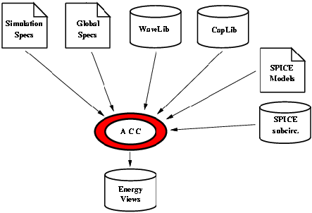
Figure 2.2: Structure of ACC.
ACC was implemented by routines written in C and scripts in UNIX C-shell, for further details see [50]. The flow of ACC is described in Table B.1
|
Source configuration file containing library paths and global parameters. For each cell in library { Create a working directory $CELLNAME. Copy in $CELLNAME the simulation specifications (sim.specs). Copy in $CELLNAME the SPICE subcircuit ($CELLNAME.sub). For each line in sim.specs (e.g. each specification) { Create SPICE netlist ($CELLNAME.spi). Write file containing simulation variables (var). For each capacitance value CL in var { For each input stimuli set specified in var { Run SPICE. Extract value (e.g. Etran) specified in var. } } Elaborate results (polynomial fitting). } Write energy view. } |
We summarize below the main features of Synopsys Power Compiler. In particular we discuss the power model, the cost function and some techniques used to reduce the power dissipation. Most of the information and data are derived from those presented in [15].
Power Compiler is built on the synthesis environment of Design Compiler and allows power optimization to be performed with delay and area optimization. Power Compiler obtains its power estimates from Design Power. The power dissipated is divided into 3 contributes:
In Power Compiler the cost function is prioritized as follows:
This means that timing constraints will not be violated to save power, but available time slack will be used to reduce it. A transformation is accepted if decreases one of the cost functions, without increasing higher priority costs.
The circuit transformations that try to reduce one of the main factors contributing to the power dissipation: gate transistor dimensions, net switching activity, net transition times and net capacitive loading are described next.
The dimensions of the transistors that compose a CMOS gate can influence a number of factors that determine the power consumption of a design. Sizing of a cell is done by choosing different implementations of the same logic function. These implementations might differ in their parasitic capacitance and internal power.
In order to reduce the switching power, Power Compiler merges or composes sets of cells into a more complex one. The switching power of the enclosed net is completely eliminated, however the internal power of the new cell is higher because of the increased gate size.
Some cells can have input pins that are symmetric with respect to the logic function (for example, in a 2-input NAND gate the two input pins are symmetric), but have different capacitance values. Power can be reduced by assigning a higher switching rate net to a lower capacitance pin.
The power due to the net transition time can be reduced by decreasing the transition times at the inputs. Power Compiler substitutes the driver of a net with a higher driver to sharpen the edge of the transition. In alternative the use of buffers can also reduce the transition time. The drawback is that the added capacitance (larger transistors in the driver, or extra gates to implement buffers) might offset the reductions obtained.
5 There are 2 transitions per clock period. Therefore, ficl is twice the frequency of the cell's clock.