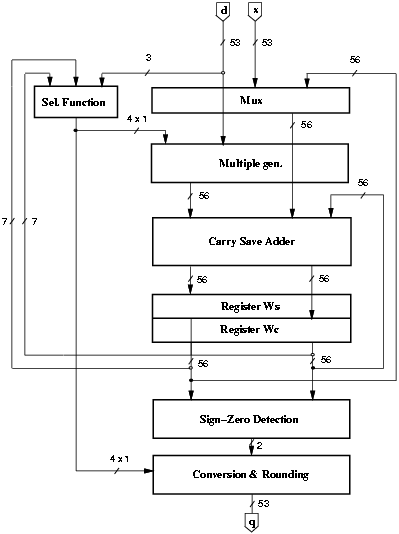
Figure 3.1: Implementation of radix-4 divider.
In this chapter we describe the techniques used to reduce the energy consumption. The radix-4 divider is presented in this chapter to establish a "standard" implementation of the digit-recurrence algorithm and better explain the application of energy reduction techniques to the unit. More detail on the implementation of the blocks is given in Appendix A.
w[j+1] = 4w[j] - qj+1d j = 0,1, Ľ, 28
with the initial value w[0] = x and with the quotient-digit selection
qj+1 = SEL(d4, [^y]) qj = {-2,-1,0,1,2}
where d4 is d truncated after the 4-th fractional bit, but only 3 bits are needed for the selection, being the most-significant bit (MSB) 1 because d is normalized. The estimated residual, [^y] = 4wS4 + 4wC4, is truncated after 4 fractional bits and with the 3 integer bits gives a total of 7 bits required by the selection function. The selection function for radix-4 and r = [2/3] is shown in Table 3.1. The quotient digit h selected is the one satisfying the expression mh Ł [^y] < mh+1. To have the divider compliant with IEEE standard for double-precision while operating with fractional values, 1-bit shifts are performed on the operands. Furthermore, to have a bounded residual in the first iteration (expression (2.3) with w[0] = x), we shift x one position to the right obtaining 54 bits for the representation of its mantissa. Since it is convenient to have the extra bit required for the rounding produced in the last position of the last digit, we shift x by an extra position to the right, obtaining a total of 55 fractional bits and 1 sign bit for the recurrence (w[j]). Each division requires 28 cycles to compute the quotient digits plus one cycle to initialize the recurrence and one cycle to perform the rounding.
| mh | dd | |||||||
| 8/16 | 9/16 | 10/16 | 11/16 | 12/16 | 13/16 | 14/16 | 15/16 | |
|
m2 | 12 | 14 | 15 | 16 | 18 | 20 | 20 | 22 |
| m1 | 4 | 4 | 4 | 4 | 6 | 6 | 8 | 8 |
| m0 | -4 | -6 | -6 | -6 | -8 | -8 | -8 | -8 |
| m-1 | -13 | -15 | -16 | -18 | -20 | -20 | -22 | -24 |
| Values in table are multiplied by 16 | ||||||||
Figure 3.1: Implementation of radix-4 divider.
The block diagram of the basic radix-4 divider is shown in Figure 3.1. The datapath shown in Figure 3.1 is completed by a controller and by a tree to distribute the clock signal (not depicted in the figure). The critical path, shown in Figure 3.2, is 7.0 ns. The energy dissipation of the unit is shown in the first column of Table 4.1 at page pageref. The largest part of the energy is consumed in the registers and in the convert-and-round unit.

Figure 3.2: Critical path for radix-4 implementation in Figure 3.1
In our approach to the reduction of the energy dissipated in the division or square root unit, we consider two main portions: the recurrence and the conversion and rounding. The following techniques are applied to the recurrence part:
For the conversion and rounding part, the following techniques are applied:
In addition we switch off not active blocks, when possible.
Most of the techniques described above do not alter the critical path and therefore do not increase the execution time of the operation performed. However, the following techniques affect the critical path:
For those techniques, tradeoffs between delay and energy consumption are considered.
The position of the registers in a sequential system affects the energy dissipation. Retiming is the circuit transformation that consists in re-positioning the registers in a sequential circuit without modifying its external behavior [20]. By retiming the recurrence we reduce the number of spurious transitions, reduce the switching activity in some blocks, and change the critical path. The retiming is done by moving the selection function from the first part of the cycle to the last part of the previous cycle (see Figure 3.3). We have to introduce a new register to store the quotient digit, but the register qj is quite small, a few bits, and it does not compromise the energy saving obtained by retiming.
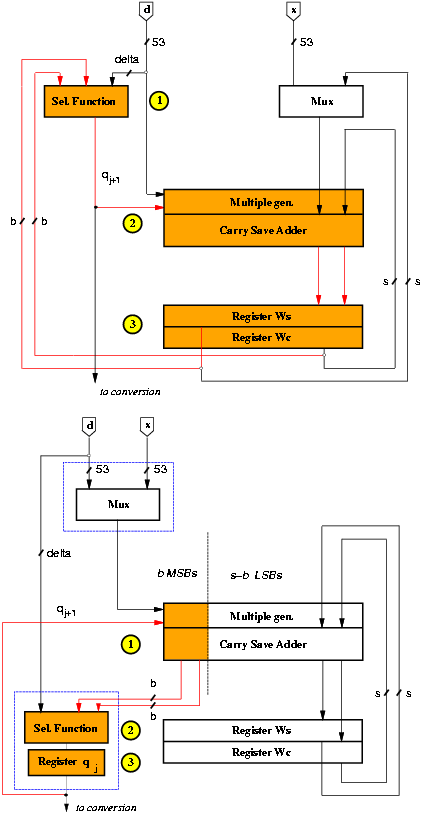
Figure 3.3: Retiming of recurrence.
Since now the quotient digit is stored in a register, this has the effect of reducing the glitches in the multiple generator and in the carry-save adder.
After the retiming, the critical path is limited to a few most-significant bits in the recurrence. Since the path through the least-significant bits of the multiple generator and the CSA does not include the selection function (Figure 3.4), these bits can be redesigned for low-power, as discussed in the next sections.
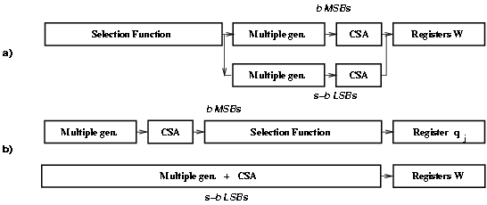
Figure 3.4: Change in the critical path. Before a) and after b) retiming.
| j | cycle | before retiming | after retiming |
|
0 | 1 | w[0] = x | w[0] = x |
| q1 = SEL(dd, r[^x]) | |||
|
1 | 2 | q1 = SEL(dd, r[^x]) | |
| w[1] = rw[0] - q1d | w[1] = rw[0] - q1d | ||
| q2 = SEL(dd, r[^w][1]) | |||
| ĽĽ | |||
|
j+1 | j+2 | qj+1 = SEL(dd, r[^w][j]) | |
| w[j+1] = rw[j] - qj+1d | w[j+1] = rw[j] - qj+1d | ||
| qj+2 = SEL(dd, r[^w][j+1]) | |||
| ĽĽ | |||
|
m | m+1 | qm+1 = SEL(dd, r[^w][m]) | |
| w[m+1] = rw[m] - qm+1d | w[m+1] = rw[m] - qm+1d | ||
| qm+2 = not used | |||
|
| |||
As shown in Table 3.2, the retiming does not increase the number of cycles needed to complete the operation.
Furthermore, by eliminating buffering for the few most-significant bits in the critical path in MULT, we can reduce the critical path (Figure 3.5).
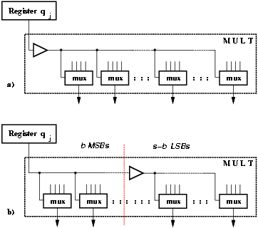
Figure 3.5: Removing buffers from MSBs.
In this modified unit, the retiming allows the re-positioning of the multiplexer out of the recurrence (Figure 3.3). In the first iteration the input x of the multiplexer is selected, while the input d is selected in the remaining iterations. The operations in the first cycle are modified by resetting register qj to 1 and allowing the input x to be stored in registers W as the first residual w[0] = 1 ·x.
The multiplexer is now in the critical path because it provides the value of either x or d to the multiple generator, which inputs are otherwise connected to the registers. However, because the output of the multiplexer is changed once per division, its delay can be masked by earlier switching. In fact, the mux-select is the only signal sent from the controller to the recurrence and it can be skewed (anticipated) at the end of the first cycle masking the delay of the multiplexer. The mux-select signal can be skewed by adding the appropriate delay (e.g. some buffers) in the distribution tree as shown in Figure 3.6.

Figure 3.6: Skewing of the
Since the contribution of flip-flops to both energy dissipation and area is significant, it is useful to change the redundant representation of the residual (wS and wC) to reduce the number of flip-flops in the registers. By using a radix-r carry-save representation with log2r sum bits and one carry bit for each digit, we can reduce the number of flip-flops. With this modification we only need to store one carry bit for each digit, instead of log2 r.
The change in the redundant representation requires a redesign of the carry-save adder to propagate the carry inside the digit (Figure 3.7).
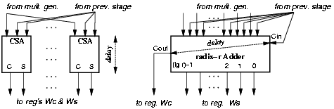
Figure 3.7: Replacing CSAs with radix-r CSAs.
In Figure 3.7, each radix-2 CSA (left in figure) is actually a full-adder (FA) implemented with two half-adders (HA). The propagation of the carry increases the delay so that this modification cannot be made for those cells (digits of w) that are in the critical path. After the recurrence has been retimed, the critical path is limited to the b MSBs. The difference between the paths through the MSBs and the LSBs is
For the LSBs in the recurrence we can redesign the CSA into a radix-r carry-save adder (r-CSA) that satisfies the following condition on delays:
|
Furthermore, because the b MSBs of the residual are assimilated in the selection function, in the retimed scheme these bits can be stored in register wS and the corresponding b flip-flops in register wC eliminated (Figure 3.8).

Figure 3.8: b MSBs assimilated in selection function.
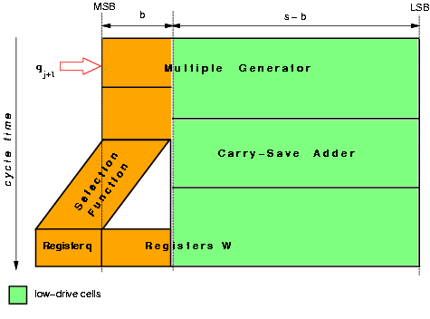
Figure 3.9: Low-drive cells in the recurrence.
Another reduction in the energy dissipation is achieved by minimizing the energy in the gates not in the critical path by using cells with lower drive capability. In the retimed recurrence, this is done for the least-significant bits (not in the critical path) of the multiple generator and the carry-save adder (Figure 3.9).
The energy dissipated in a cell depends on the square of the voltage supply (VDD) and a significant amount of energy can be saved by reducing it [14]. However, by lowering the voltage the delay increases, so that to maintain the performance this technique is applied only to cells not in the critical path. Different power supply voltages require level-shifting circuitry that contribute to the total energy dissipation. As a consequence, it is convenient to apply this technique only if the number of cells not in the critical path is quite large, and the energy increase in the level-shifting circuitry does not offset the reduction due to voltage scaling. However, by using two voltages we only need to level-shift when going from the lower to the higher voltage [35]. A more complete description of the level shifter for dual voltage is presented in Appendix A.
In the case of the divider, as shown in Figure 3.10, the s-b least-significant bits, can be redesigned for low-voltage. The voltage-level shifters are not needed until a specific digit moves towards the b-MSBs, by shifting across iterations, and into the critical path. By placing the voltage-level shifters in the digit immediately before the b-MSBs the cycle time is not increased. In order to evaluate the possible lower voltage V2 to be used in a dual voltage implementation we need to determine the time slack available for the LSBs. The time slack is the difference between the delay in the paths through the MSBs and LSBs, and it gives the amount of time available for the delay of gates whose voltage is scaled to V2.

Figure 3.10: Low-voltage cells in the recurrence.
The delay of the least-significant portion depends on the type of CSA adder used, since the delay of the radix-r CSA is larger than that of the radix-2 CSA. Since the reduced voltage can be lower for radix-2 CSA, this might result in a reduction of the total energy. There is a tradeoff between the following:
By equalizing the paths of the input signals of the blocks we reduce the generation of glitches [16]. Because of different delays, both gate and interconnection delay, the input signals to the carry-save adder (CSA) arrive at different times, creating spurious transitions inside the adders. For instance, Figure 3.11 shows, in the upper part, a possible implementation of one of the full-adders composing the carry-save adder. Pins a and b are directly connected to the registers, whereas pin d is connected to the output of the multiple generator. If the input signals a and b arrive at different times, glitches might be produced in e and f. Also, if there is a difference between the arrival times of d and e, glitches might be produced in S, g and C.
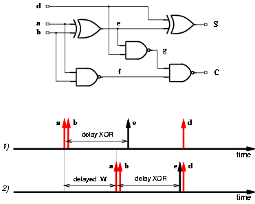
Figure 3.11: Equalizing paths in CSA.
Time diagram 1) in Figure 3.11 shows an example of the distribution of the arrival times for signal a, b, d, and e. In order to eliminate the spurious transitions, we delay the clock to the Ws and Wc registers (which produce a and b) so that the signals e and d, overlap, as shown in time diagram 2) in Figure 3.11. However, it is impossible to eliminate all the glitches because due to the different delays of the XOR and NAND gates, signals at nodes f and g always arrive at different times.
The quotient-digit selection is a function of a few bits of the divisor and of the residual. Since the divisor is fixed for the whole division operation, from the point of view of energy consumption it is convenient to decompose the function into subfunctions and to enable only the subfunction corresponding to the actual value of the divisor. This is specially convenient for higher radices, because the quotient-digit selection is more complex and therefore is responsible for a significant portion of the energy.
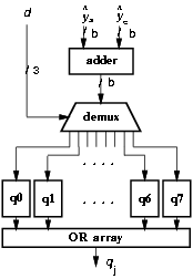
Figure 3.12: Partitioned selection function.
Figure 3.12 shows an example (d = 3 bits of the divisor are required) in which the selection function is partitioned in 2d = 8 parts (all the possible values of d3). The demultiplexer transmits the assimilated value of [^y] to the selected pair of selection tables and forces to zero the output of the others. Finally an array of OR gates concentrates again the value of the quotient-digit.
Experimental results showed that the partioned selection function dissipates less energy, but because of the demux and the OR gates the critical path increased.
In the retimed implementation, the selection function is connected to the output of the carry-save adder, instead of directly after the registers (Figure 3.3). As a consequence of its repositioning, there is an increase in the number of glitches in the selection function. One way to filter those glitches is to buffer the selection function with multiplexers acting as latches, as described in Figure 3.13.
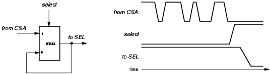
Figure 3.13: Glitch suppression using multiplexers.
The select signal is driven by a different clock (same period, different phase) that enables the multiplexers to transmit the value from the CSA when it is stable, and hold the current value otherwise. However, in this case the delay of the multiplexer affects the critical path. More precisely, the additional delay in the critical path is due to two contributions:
This second contribution can be eliminated by triggering the select signal before the output of the CSA is stable. However, in this case, some glitches might not be suppressed.
In the conversion and rounding part of the divider, we both modified the algorithm and applied gate-level energy reduction techniques.
We now describe the modifications in the conversion algorithm for the two cases: a < r-1 and a = r-1.
When a < r-1, in the original algorithm, two registers (n bits each) are needed to store Q and QM. The registers are filled with digits starting from the least-significant position and then shifted towards the most-significant position. The large number of flip-flops used and the shifting result in a large energy consumption in the convert-and-round unit.
As a first step to reduce the energy dissipated, we load each digit in its final position. In this way we avoid the need to shift digits along the registers. To determine the load position we use an m-bit ring counter. The algorithm starts the computation from the most-significant digit. In iteration j
As a second step, we eliminate register QM. When qj < 0 it is necessary to propagate a borrow. In the original algorithm, QM is used to avoid this propagation. Instead of the register, to propagate this borrow (without actually doing the subtraction) the digits which change because of this propagation are marked. These digits correspond to the last sequence of zeros plus the last nonzero digit before this sequence. These are marked by the same ring counter by keeping a 1 for those digits that might be changed by a borrow.
We refer with Q[i] to the digit position in the register Q and with C(i) to the bit position in the ring counter (Figure 3.14). The modified algorithm is shown in Table 3.3.
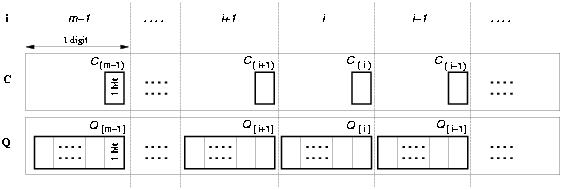
Figure 3.14: Registers C and Q in the new converter.
| If qj > 0 | then Q[i] Ü qj | |||||||||||||
|
| AND set C(i-1) Ü 1 AND reset all other bits in C | |||||||||||||
|
If qj = 0 | then Q[i] Ü 0 | |||||||||||||
|
| AND set C(i-1) Ü 1 /* no resetting in C */ | |||||||||||||
|
If qj < 0 | then Q[i] Ü r - \mid qj \mid | |||||||||||||
|
| AND { |
| ||||||||||||
| AND set C(i-1) Ü 1 AND reset all other bits in C | ||||||||||||||
The updating expression for the ring counter is
| (14) |
Table 3.4 shows how the conversion is modified, for the example presented in Table 2.1.
| j | qj | Q | C | |||||
| 1 | 1 | 1xxxxxxxx | 010000000 | |||||
| 2 | 2 | 12xxxxxxx | 001000000 | |||||
| 3 | 0 | 120xxxxxx | 001100000 | |||||
| 4 | -1 | 1133xxxxx | 000010000 | |||||
| 5 | 0 | 11330xxxx | 000011000 | |||||
| 6 | 0 | 113300xxx | 000011100 | |||||
| 7 | 2 | 1133002xx | 000000010 | |||||
| 8 | -2 | 11330012x | 000000001 | |||||
| 9 | -1 | 113300113 | 100000000 | |||||
In the final rounding, the last digit is loaded with pt as in expression (2.4). If the last digit is negative the update (to propagate the borrow) is done as in the other iterations. The only exception is when qm = -1, and by rounding it p = 0 is obtained. In this case, the register Q is not updated.
When a = r-1 three registers Q, QM and QP are needed for the conversion and rounding (Section 2.2). The register QP is eliminated by recoding the quotient digit into the digit set { -(r-1), Ľ, -1, 0, 1, Ľ, r-2}. The value r-1 is recoded into -1 and the previous digit incremented by one. This recoding requires to store the current quotient digit in a temporary register T (log2 r bits + 1 sign bit) as sketched in Figure 3.15. No additional cycle is needed since the conversion of the last digit is done together with the rounding. Table 3.5 shows an example of conversion, for radix-8 and a = 7, using this recoding.
With the implementation of the new algorithm we reduce the number of flip-flops in the convert-and-round unit from 2n to (1+[1/(log2r)])n when a < r-1 and from 3n to (1+[1/(log2r)])n + log2r+1 when a = r-1.
Summarizing, the algorithm is modified by eliminating the shifting of the digits previously loaded and by replacing registers QM and QP with two additional, but smaller registers: C, which is introduced to keep track of the digits to update, and T, which is used for the recoding.

Figure 3.15: Use of register T.
|
qj | T | Q | C | ||
| 4 | 4 | xxxxxxxx | 10000000 | ||
| 7 | -1 | 5xxxxxxx | 01000000 | ||
| -1 | -1 | 47xxxxxx | 00100000 | ||
| 7 | -1 | 470xxxxx | 00110000 | ||
| 0 | 0 | 4677xxxx | 00001000 | ||
| 7 | -1 | 46771xxx | 00000100 | ||
| 7 | -1 | 467710xx | 00000110 | ||
| 7 | -1 | 4677100x | 00000111 | ||
| Final rounding | |||||
| add 1 | x | 46771000 | 00000111 | ||
| add 0 | x | 46770777 | 00000111 | ||
As a further step to reduce the energy dissipation in the convert-and-round unit, we switch off the clock signal for the flip-flops in the register that do not have to be updated. Figure 3.16 shows an application of the gated flip-flop technique [19]. We introduce the activation function F, that enables the clock of the flip-flop only when it is needed. As described in [19], F must be ANDed with the clock signal (clk) for trailing-edge-triggered flip-flops. For leading-edge-triggered (rising edge) flip-flops an AND gate cannot be used, to avoid a malfunctioning of the circuit if the delay (d) of F is shorter than the period the clock is high (h), as shown in Figure 3.16.a (d < h). By making the flip-flop clock signal
| (15) |

Figure 3.16: Gated flip-flop enabling function.
With this technique, in the ring counter (refer to Figure 3.14) the clock of flip-flop C(k) is enabled when
The resulting enabling function is
|
|
|
|
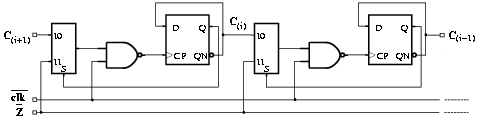
Figure 3.17: Two consecutive bits in the ring counter.
In register Q, the current digit is presented to the input of all the flip-flops, but only the digits modified at that iteration are loaded, by enabling the clock signal of the corresponding flip-flops. If at start-up register Q is initialized to 0, no load is needed when qj+1 is zero. The clock signal of digit Q[i] is enabled when
The enabling function E[k] is
|
| (16) |
| ||||||||||||
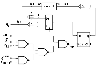
Figure 3.18: Clock enabling function and loading in register Q.
The modified conversion algorithm requires that the converted quotient digit be presented to the full array of flip-flops in register Q, and then, only log2r of them are loaded with this digit. To distribute the digit and the clock we need a tree (Figure 3.19.a) that dissipates a significant amount of energy. Because of the particular structure of the algorithm, by dividing the register Q into two portions, upper (m/2 most-significant digits) and lower (m/2 least-significant digits), we can switch-off a part of the tree for half the number of the iterations. This is obtained by dividing the tree into two halves and by propagating the signal to the upper array of flip-flops when executing the first m/2 iterations and to the lower array in the rest as shown in Figure 3.19.b. Signals AU and AL = [`AU] select the half array to feed and g represent a generic bit to be loaded in the flip-flops. To keep track of which part of the array is computed we use an additional flip-flop that is set after the m/2-th iteration. By implementing this gated-tree we can save about 50% of the energy dissipated to distribute the signals (the gates introduce extra capacitance, and also the number of transitions are not equally distributed in the two portions of the array).
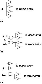
Figure 3.19: Gated tree. a) before, b) 50% reduction,
On the other hand, when computing the digits in the lower portion we might need to update the digits in the upper array, for this reason we cannot switch-off the clock (for example) for the upper part. But the clock can be disabled for the lower part in the first m/2 iterations. In this case the reduction is about 25% (Figure 3.19.c).
As a further refinement, we can switch-off the clock and digit-sign in the upper part after a digit different from 0 has shown up in the lower array. This requires an additional flip-flop to mark the state ßecond part of the array and digit different from zero occurred".
Because the convert-and-round unit is not in the critical path, we can use low-voltage cells to realize it. The number of level-shifter required is n: one for each bit of the final quotient that must be raised from the lower voltage to the higher (VDD). Note that in the last cycle of the division, when the result is produced, the larger delay of the low-voltage flip-flops will produce q at a later time than in the non-reduced voltage implementation.
The modification consists in switching-off blocks which are not active during several cycles. This is the case for the sign-zero-detection block (SZD), which is only used in the rounding step to determine the sign of the final remainder and if it is zero. The SZD can be switched off by forcing a constant logic value at its inputs during the recurrence steps (Figure 3.20).

Figure 3.20: Disabling SZD during recurrence iterations.
Logic synthesis provides the automatic synthesis of gate-level netlists, optimizing the design for various constraints. The solution of an optimization problem is measured in terms of a cost function [36]. The cost measures the extent to which a constraint has been met. If the constraint has been satisfied, the corresponding cost is zero. A different priority is given to the constraints, for example:
This means that timing constraints will not be violated to save power, but available time slack will be used to reduce it. A transformation is accepted if it decreases one of the cost functions, without increasing higher priority costs.
In order to minimize the energy, or power dissipation, determined either by probabilistic estimation algorithms or by gate-level simulation, circuit transformations that try to reduce one of the main factors contributing to the energy consumption (gate capacitance, net switching activity, net transition times and net capacitive loading) are applied to the design.
In our case, we used Synopsys Power Compiler, which performs synthesis at gate-level with optimization capability for power dissipation. The main features of the tool, derived from [15], are briefly discussed in Appendix B Section B.3. The synthesis is performed on relatively small blocks as explained in Chapter 4.